Microcap Simulation
This page contains some basic idea for some implementations using Microcap that was taught in my sixth semester at IIT Kanpur.
[ESC201P] Microcap elements
-
adding dependent sources : component -> analog primitive -> dependent sources
-
adding sliders: run dynamic DC analysis -> dynamic dc tab -> add slider
-
add diode: we choose diode In4001
-
add bjt: we choose 2N2222
-
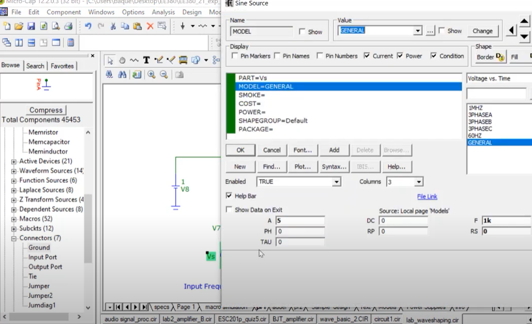
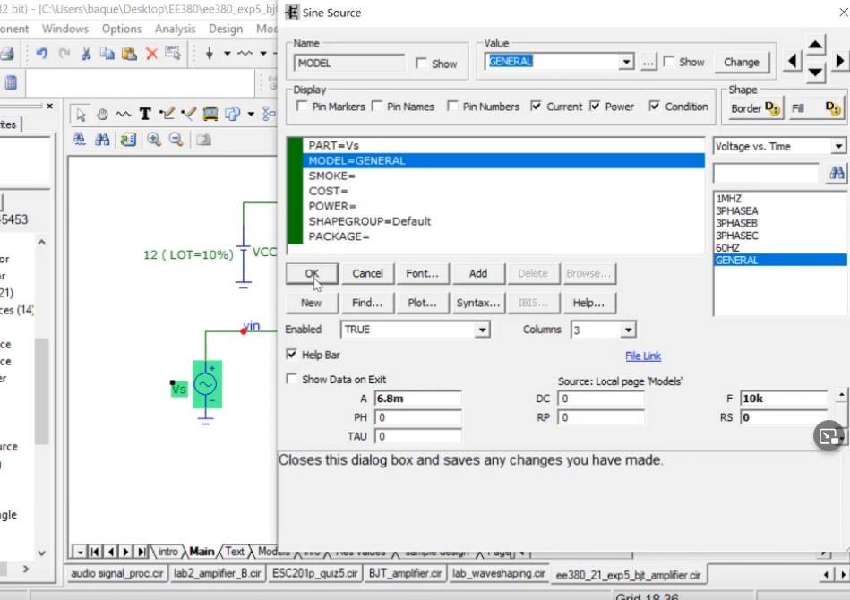
add AC source: left panel -> analog primitives-> waveform sources-> sine source -> general(type)
-
add audio signal: left panel -> analog primitives-> waveform sources-> WAV file source
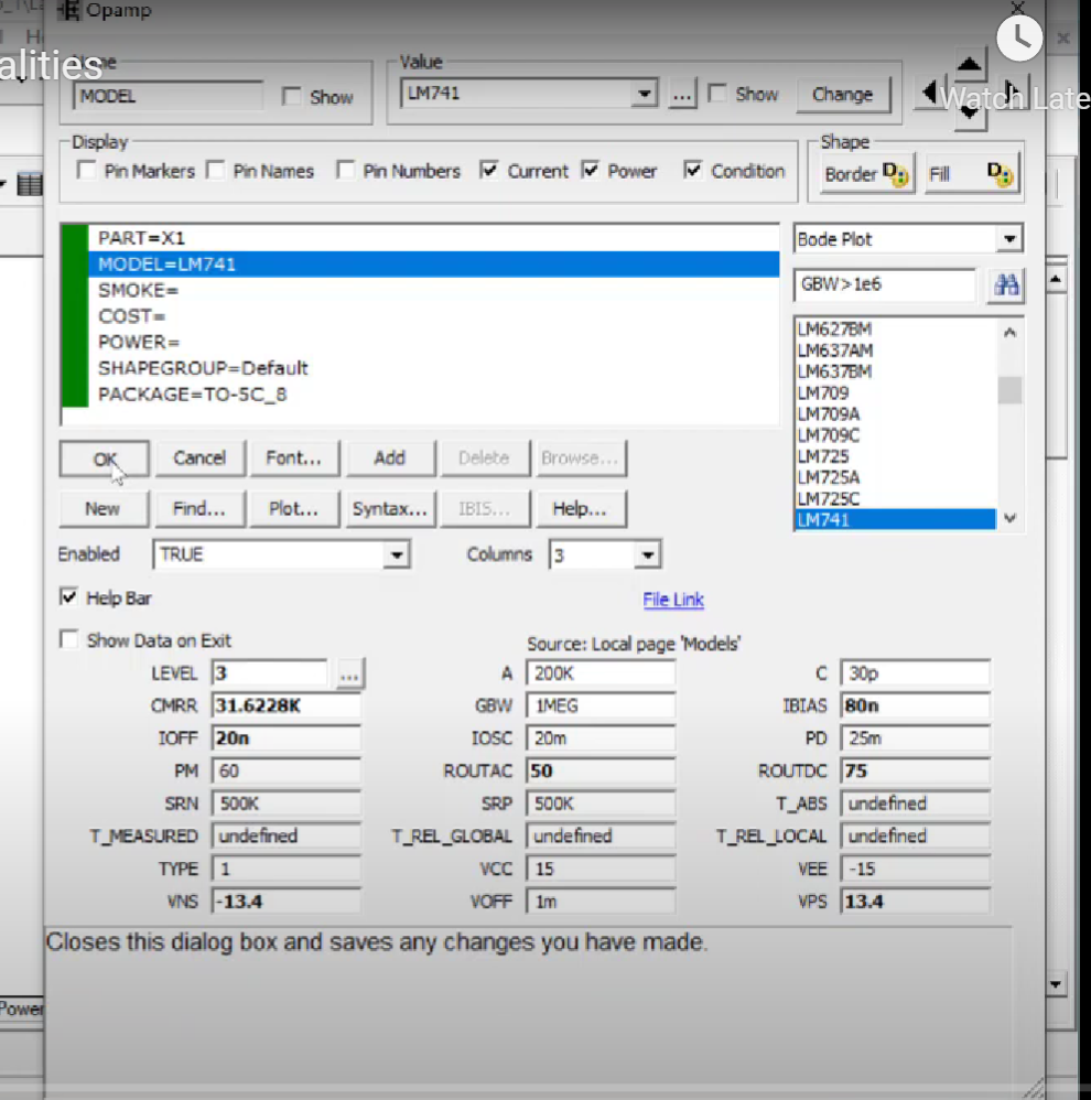
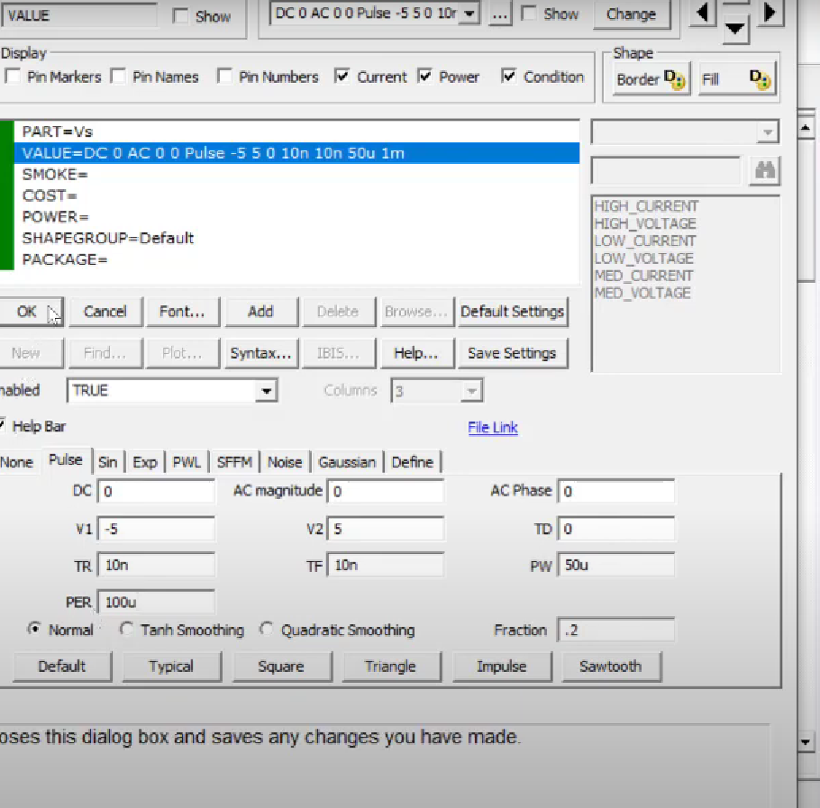
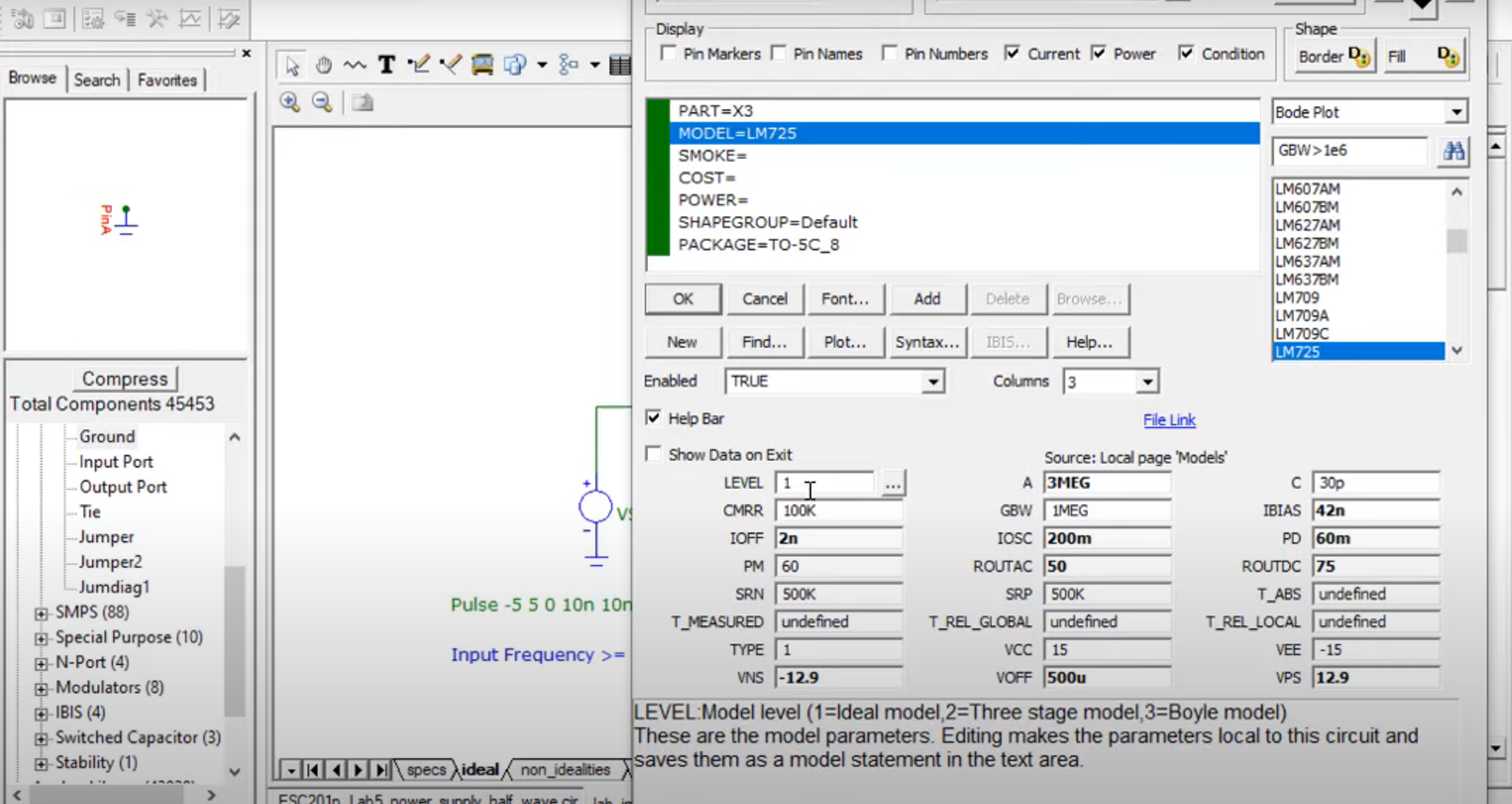
opamp: use OPAMP from analog primitives -> active devices -> model LM741 and level = 3 -
BJT: LEFT PANEL -> ANALOG LIBRARY -> GENERAL -> BC548(then change it to BC547)
-
digital primitives -> standtard gates stimulus generators -> inputs to the gates
choose fixed stimulus
time varying commands
.define _100MHZclk
+0ns 0
+label = start
+50ns 1
+100ns 0
Models available in Labs(IITK-Labs)
*OPAMP : Value LM741
*Sinusoidal Source: Value General
*Use transistor BC 54
Info (link)
Dynamic DC Analysis
Performs DC analysis on the system and changed the component dynamically as we change it in the simulation. We also get an option to add a slider for changing the value of a component
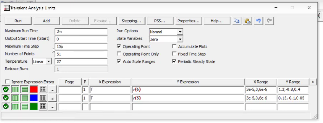
Transient Analysis
Useful for circuits that vary with time(generally due to capacitors). We can set maximum rum time, maximum step time and other limits and perform transient analysis.
AC Analysis
This plots the transfer function of the output with respect to the input(assuming the input to be 1, that is basically plots the ratio). We can set the frequency range, limits and perform the AC analysis.
DC Analysis
Allows us to see how one parameter changes with others, if we sweep something(generally on x-axis) at some range.
Understanding Non-Idealities of Opamp (link)
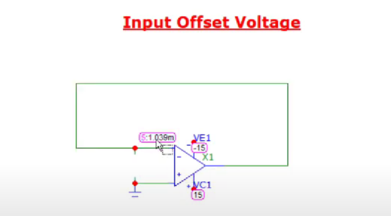
This is a Level-3 Opamp(which perfectly reflects actual Opamps)
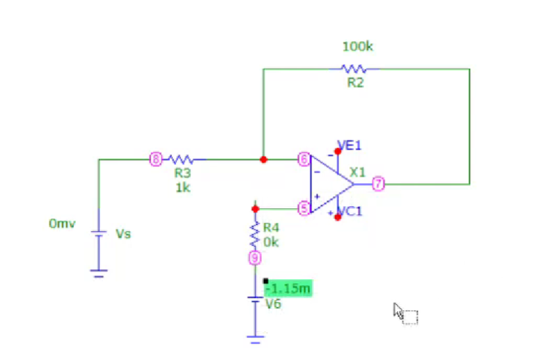
Input offset Voltage: Ideally both the terminals of Opamp should be at same potential(virtually grounded), but there is a bias voltage present in between them.
Input offset current: Difference in the bias current flowing in the non inverting terminal(ideally it should be 0)*
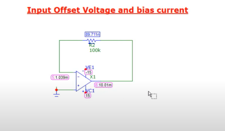
Fine tuning these biases can be done by adding some resistances or voltages over the inverting terminal
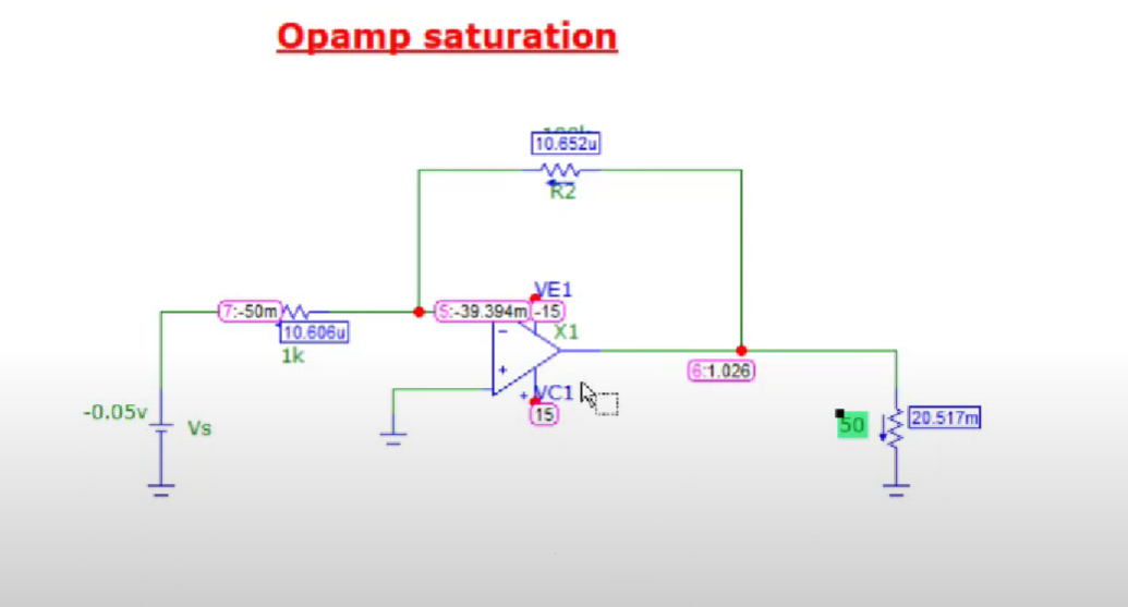
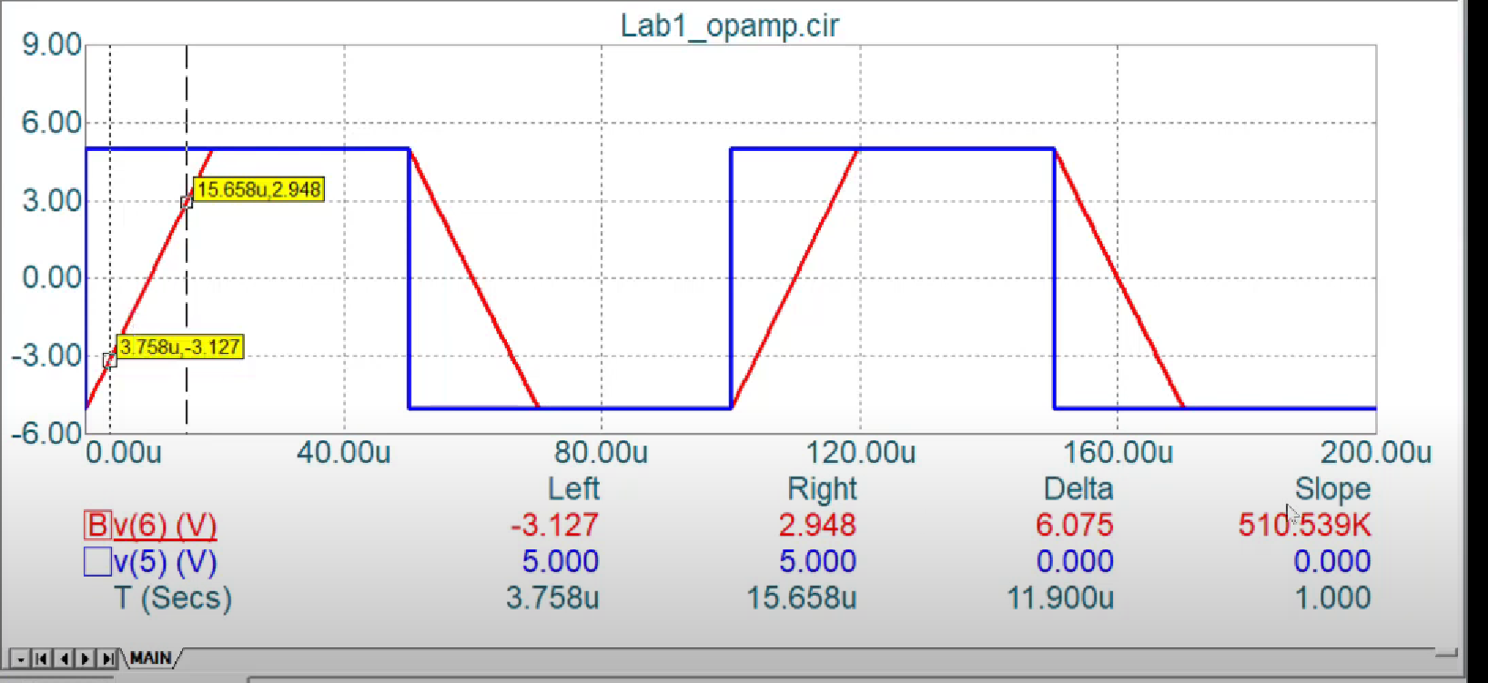
Opamp Saturation: The maximum voltage that the OPAMP can achieve is equal to that of power supplies attached to it. There is also a limit over the maximum current that the OPAMP can supply as can be seen below.
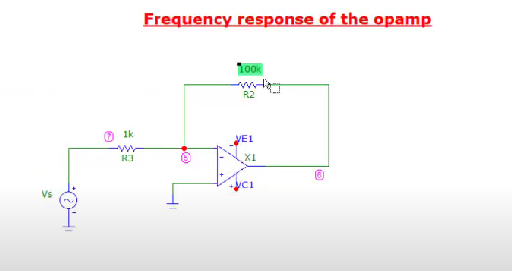
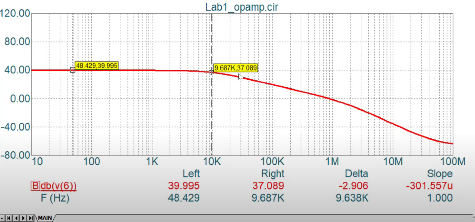
Frequency response of OPAMP: There is frequency response assosiated with OPAMP(behaves as low pass filter). This response does not allows perfect $180 deg$ phase shift and gain to be reflected to the ouput on connecting an sinusoidal input.
The maximum frequency that the OPAMP operates on can be found by connecting a gain of $1$ to the opamp and then finding out the $3dB$ drop point(Put $R_2 = 1$, and then find out the $3dB$ point). We can only amplify signals which are less than this unity gain frequency. But, if we go to higher gain the frequency starts detoriorating at earlier frequencies because of this gain bandwidth product.
Slew Rate : On higher frequencies, OPAMP dont seem to follow the input perfectly. There is a rise and fall time assosiated with it as can be seen below. This also depends on the input of the voltage source. We can see this affect primarily over larger voltage and larger frequecny values.
Noise in Circuits (link)
Increasing gain in the opamp circuit
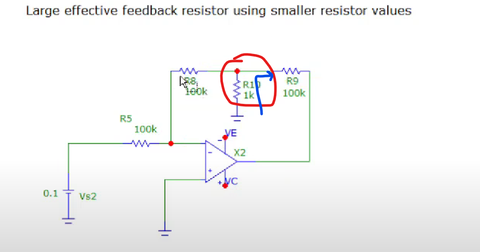
One way is to connect high resitances and thus increase the gain, but such high resistances are often not feasible, thus we try to increase the current in the branch. This is achieved by connecting smaller resistances which creates negative potential and allows more current to flow in.
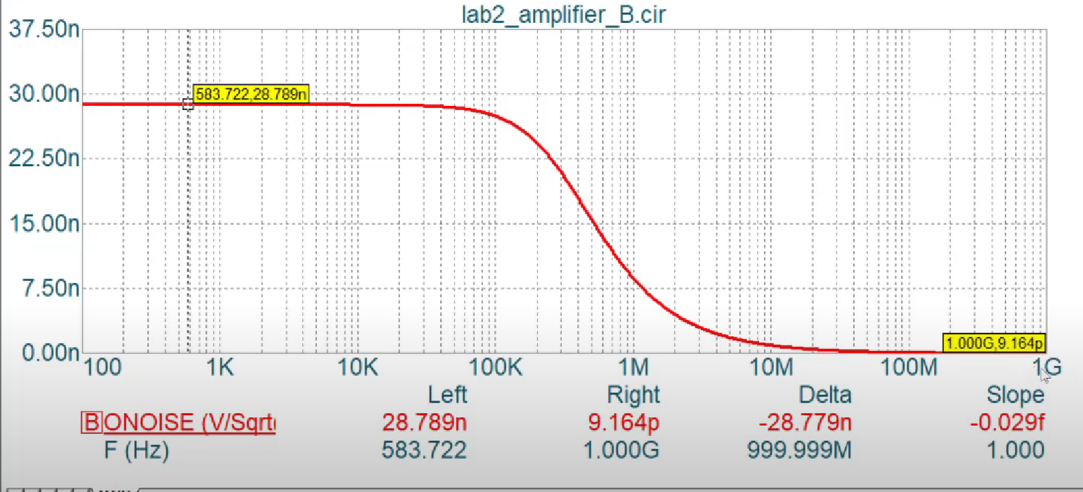
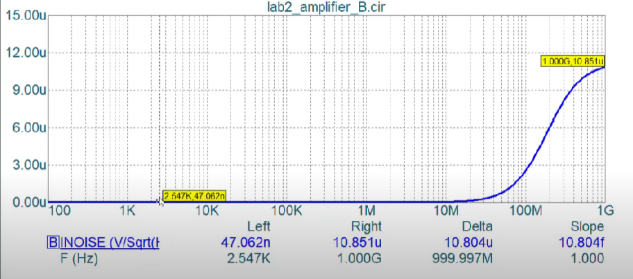
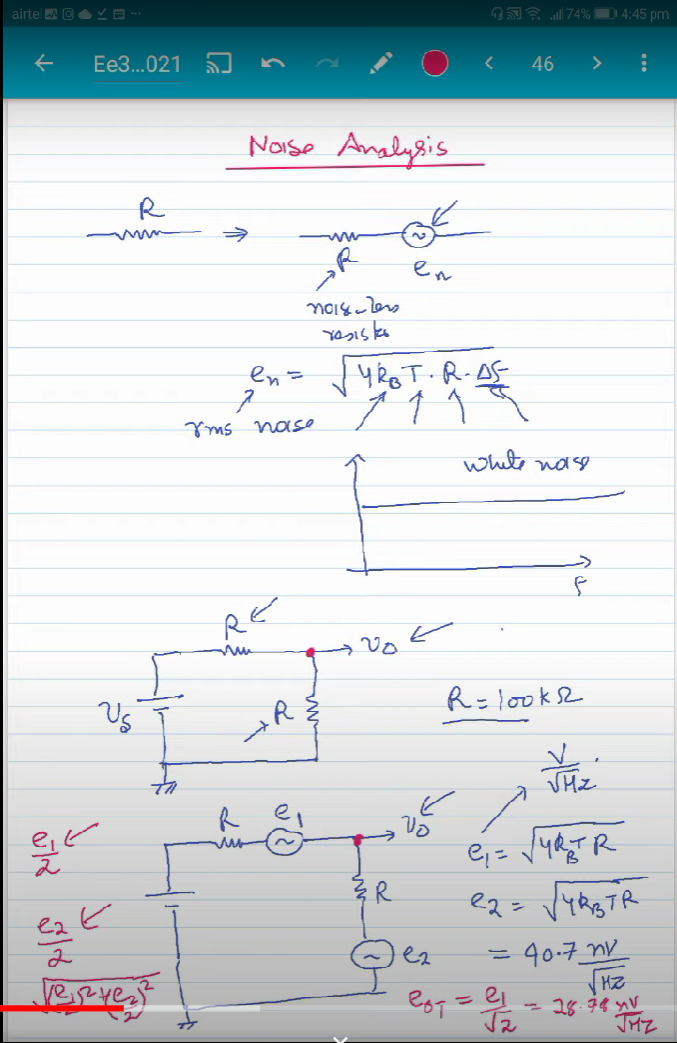
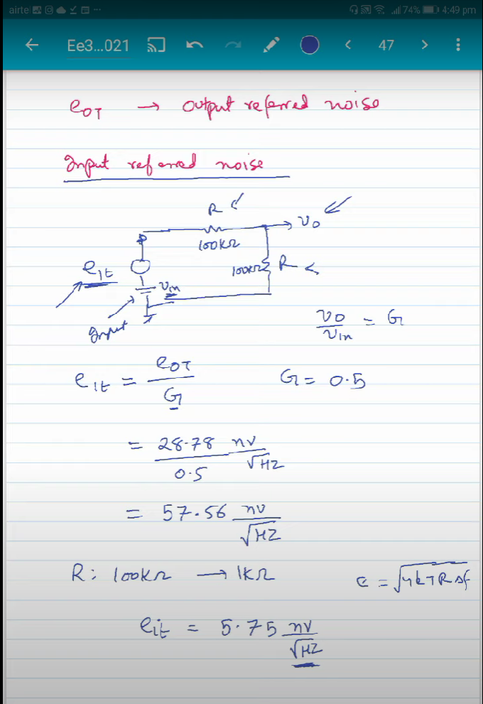
Noise Analysis
Most of the components in the circuit generates noise. Diodes, Mosfets, BJTs, resistors they all generate noise in the circuit.
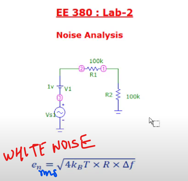
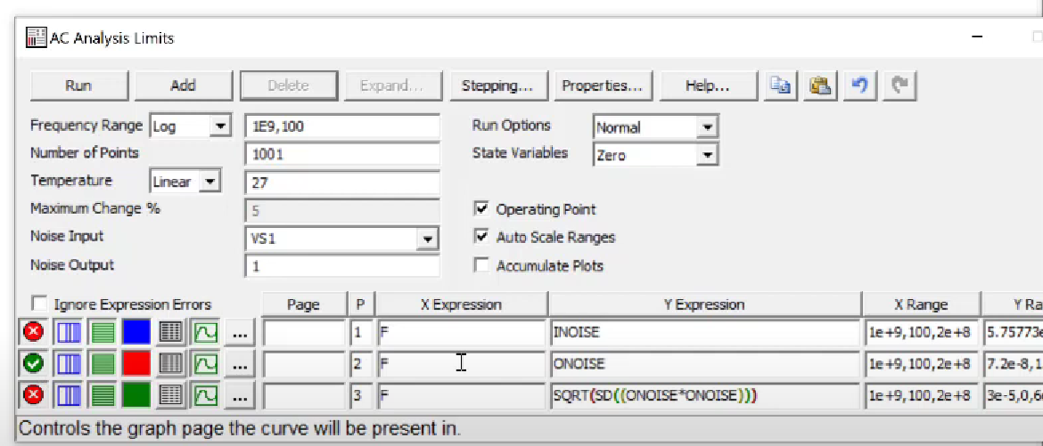
Noise Analysis using Microcap is done in AC mode.
Circuit with resistor
We can see that the output noise is a White noise.
The noise is also tranferred back to the input and is called as input noise.
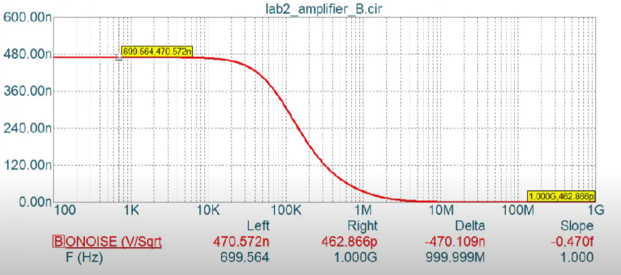
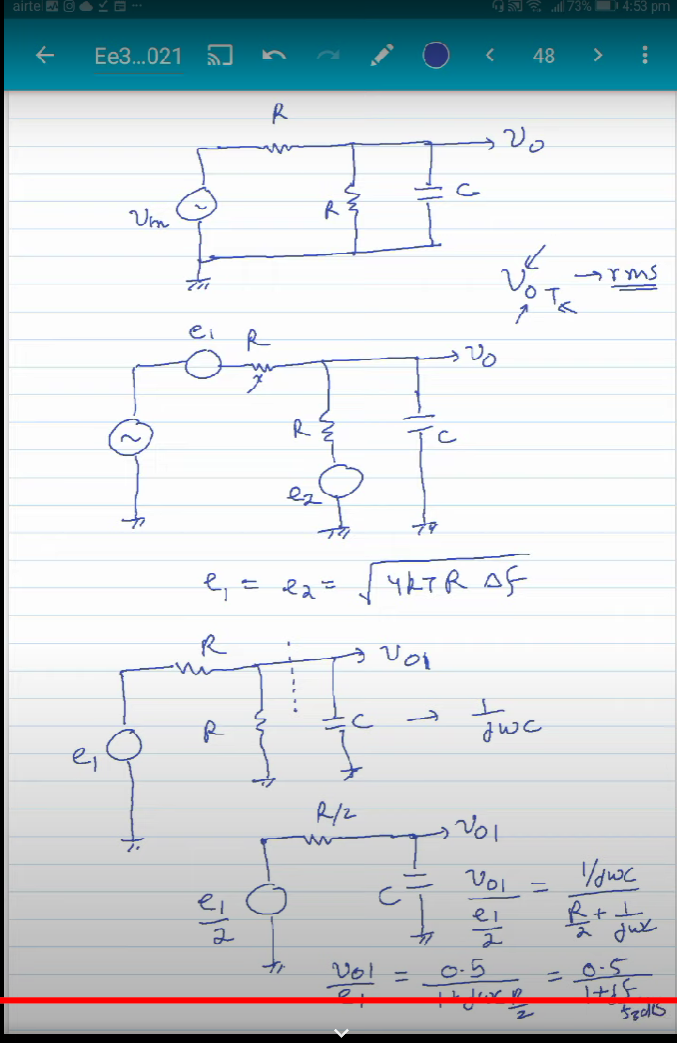
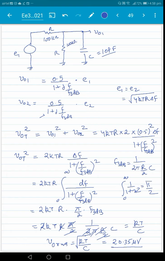
Circuit with resistor in parallel with a capacitor
On adding a capacitor in parallel to the resistor as shown below,
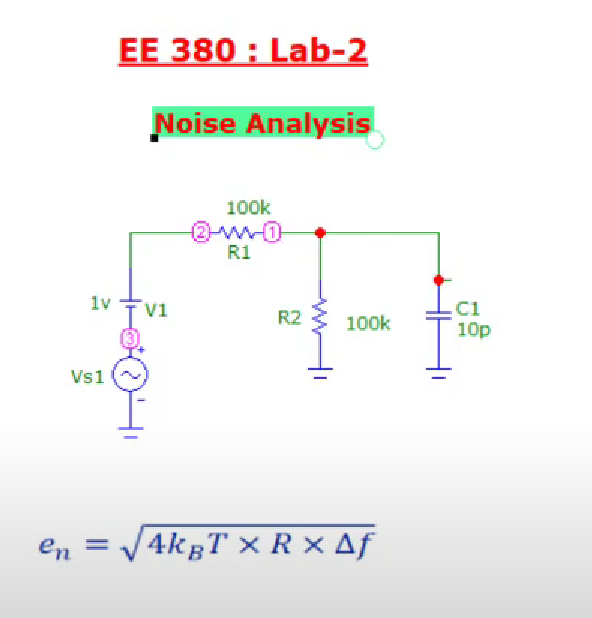
we, get the following output noise
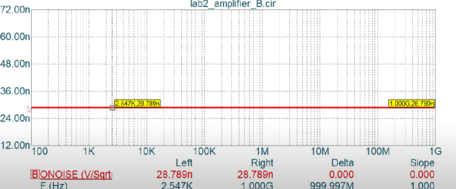
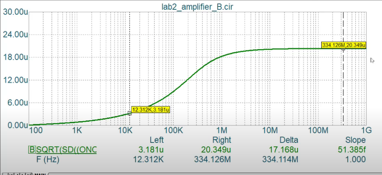
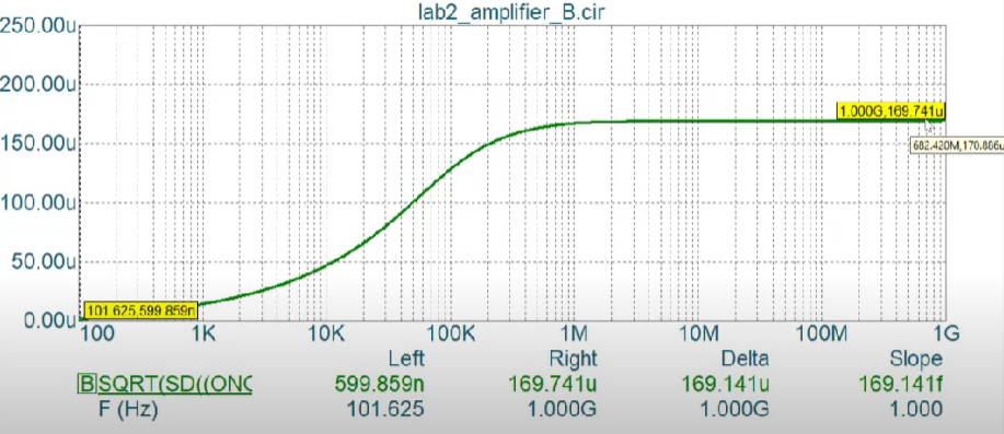
To get the total noise from the above graph, we need to integrate it over all the valuws. This can be achieved in microcap by plotting the following graph. This is achieved by using $sd$, which does the work of integration.
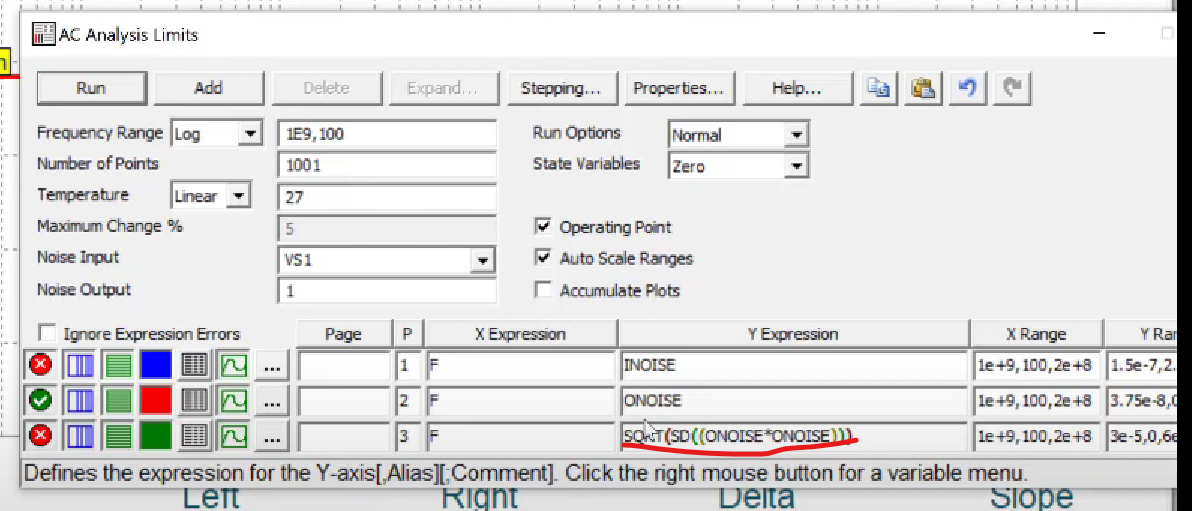
The steady state value is the total rms value of the noise generated.
Opamp Circuit
We are neglecting the noise present in LM741 opamp model
We can also find noise for the following circuit
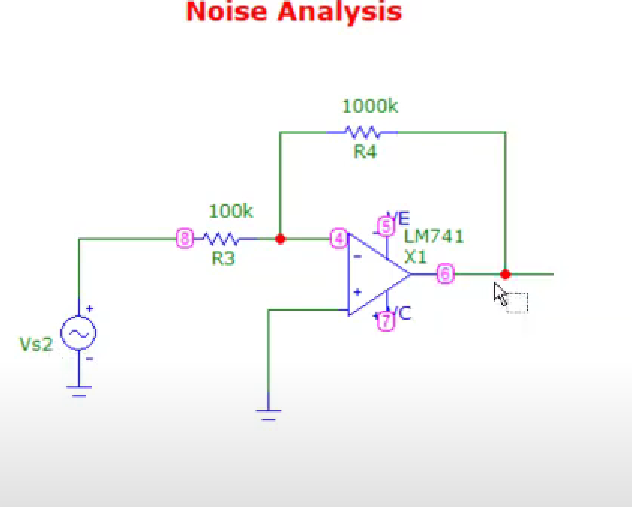
The noise referred at the input looks like the following
The noise at the output looks like the following
The total noise upon integration can be found in the same manner as in previous case.
Mathematical Analysis for Noise(link)
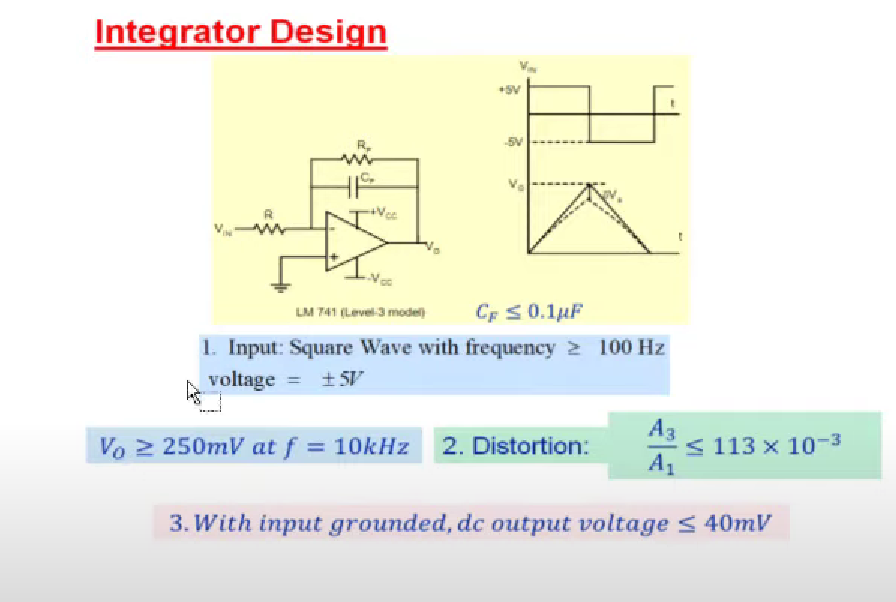
Design of an integrator (link)
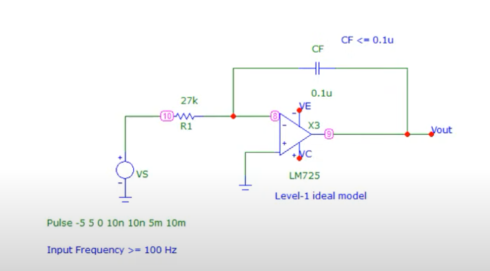
Ideal integrator
First of all we build an ideal integrator and then tune it to add the non idealities.
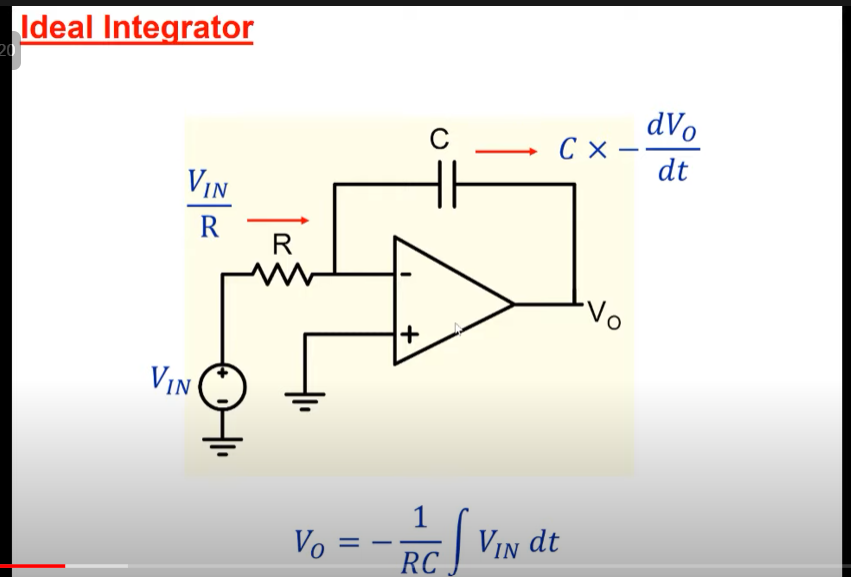
The ideal integrator we choose is a level1 integrator as shown in the figure.
Following constraints of Capacitance and frequecny should be met to keep the circuit compact.
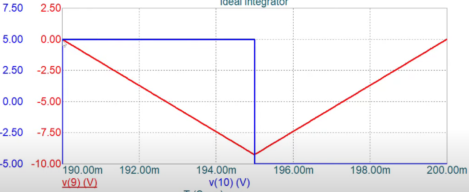
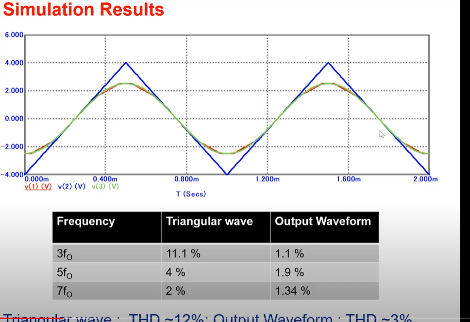
Now, we try to observe the output of this input in the last $10ms$, as it’s time period is $1/100$ and some transient behaviour requires some time to settle down.
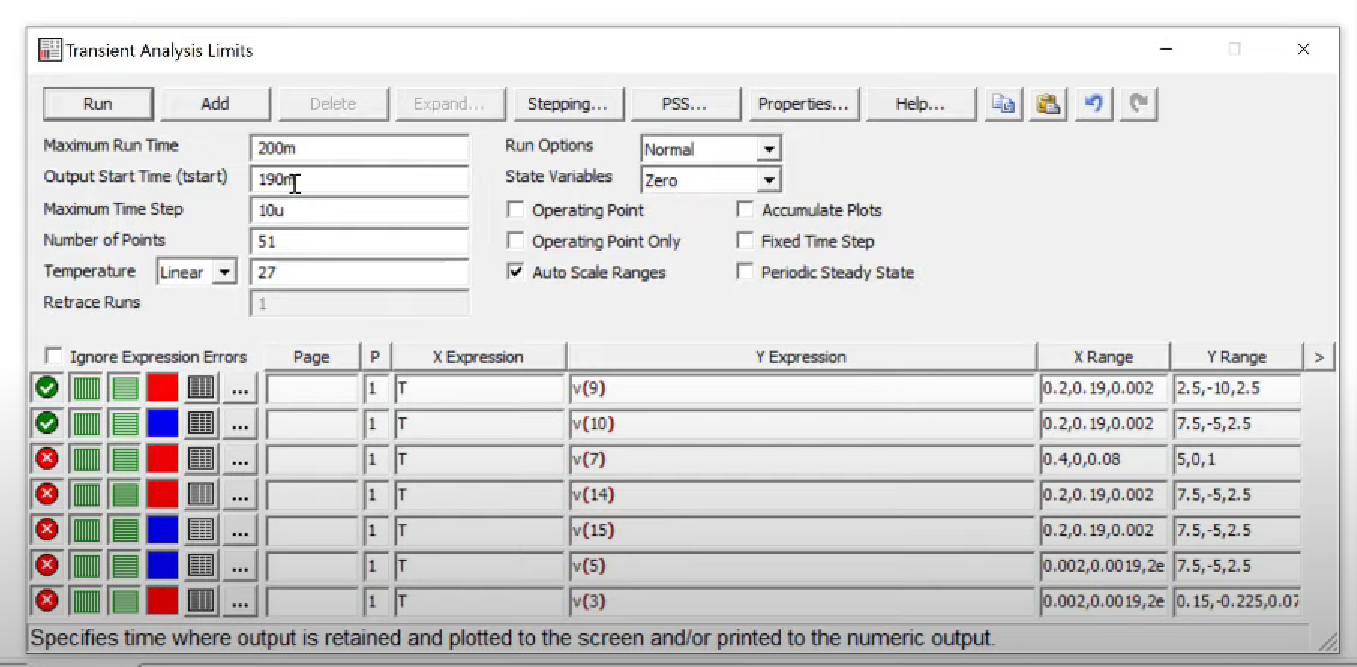
The result is as follows
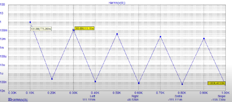
To observe the idealities, we may add a fourier window using the transient tab in the graph
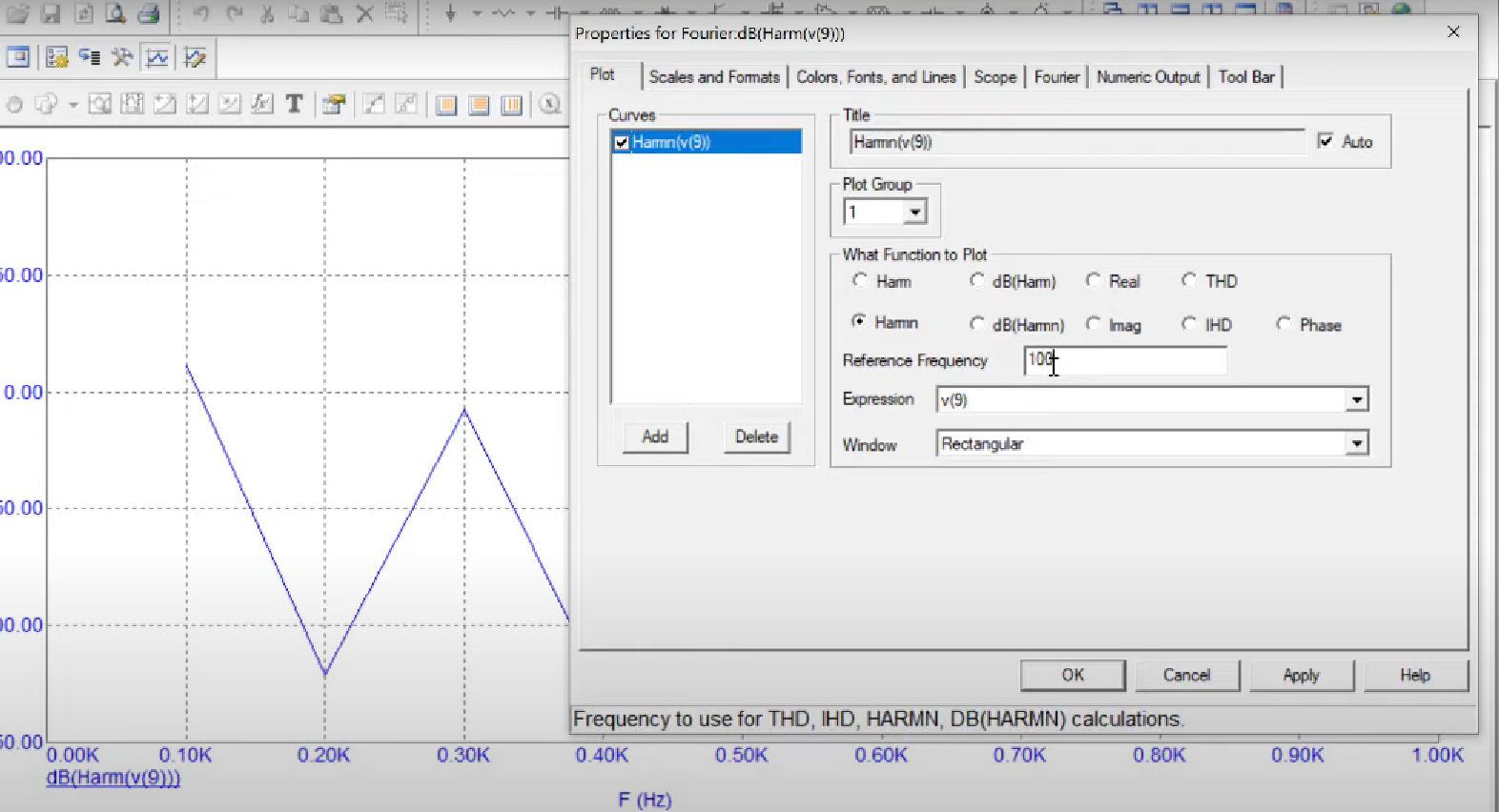
The result should be something like the following where the amplitudes of harmonic are in the following manner
Non-Ideal integrator
The opamp tends to output some voltage even if no input voltage is applied.
We add resistor in parallel to prevent non-idealities and thus
prevent saturation.
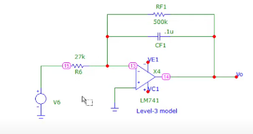
But now the integrator becomes non ideal
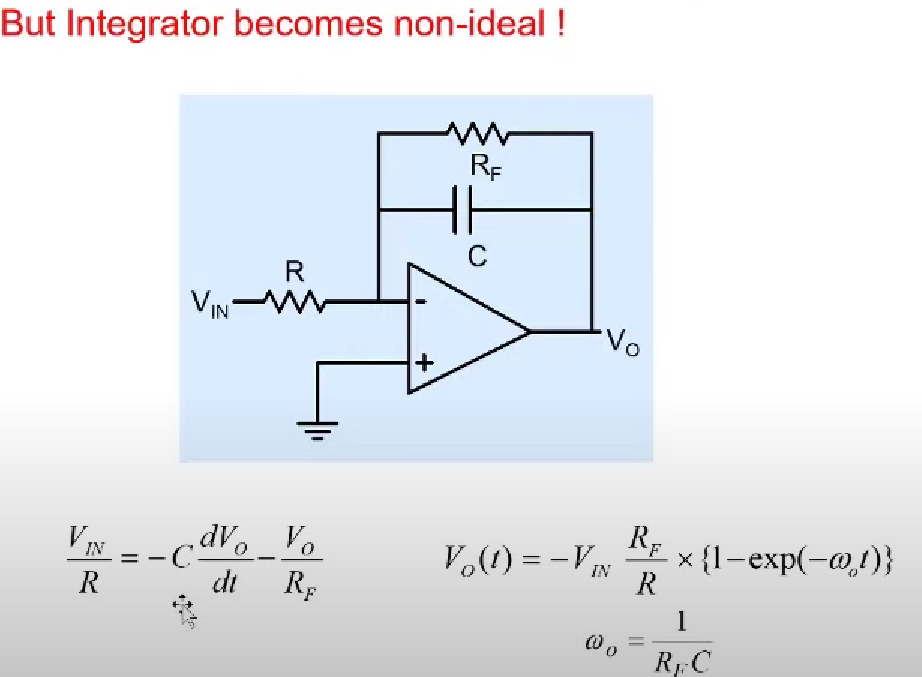
Following are the issues when we try to make it into ideal integrator
- The Dc offset depends on the gain of the circuit(RF1/R6). Reducing gain reduced Dc Offset but the integrator gets distorted(third harmonics starts changing in the fourier window).
- Thus we need to keep RF1 on higher side but that increases offset voltage. We may try to increase R6 but though this reduces the gain, it also decreases the amplitude of the traingular wave.
Required specs are as
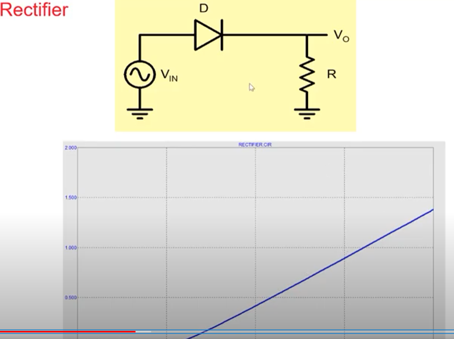
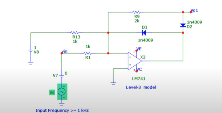
Wave Shaping (link)
We will generate a triangular input and then pass it through another circuit to generate a sinusoidal wave. The other circuit’s threshold can be adjusted to reduce distortions.
We will be designing the other circuit by breaking it into three parts as shown below:
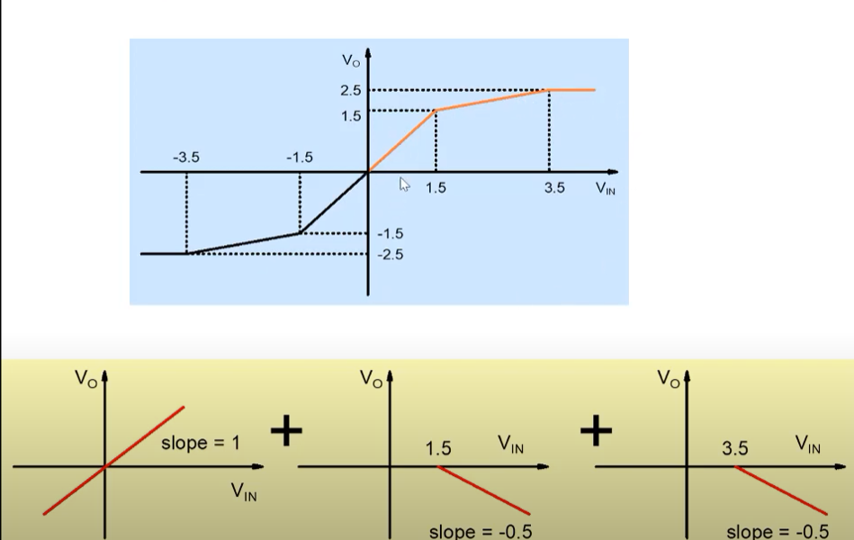
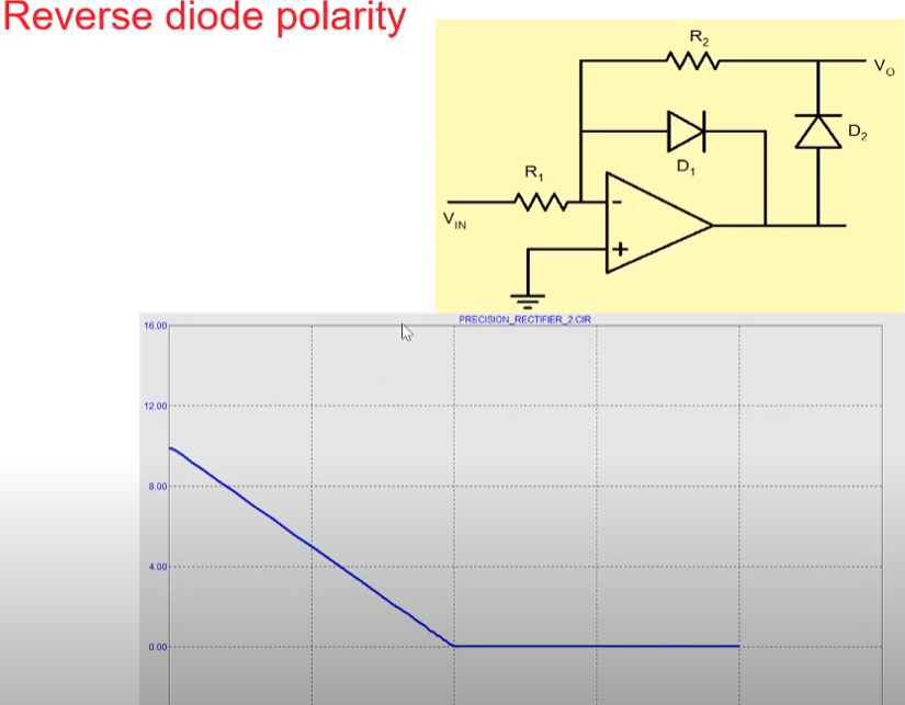
The first figure can be generated easily using a wire while the others can be done using a rectifier
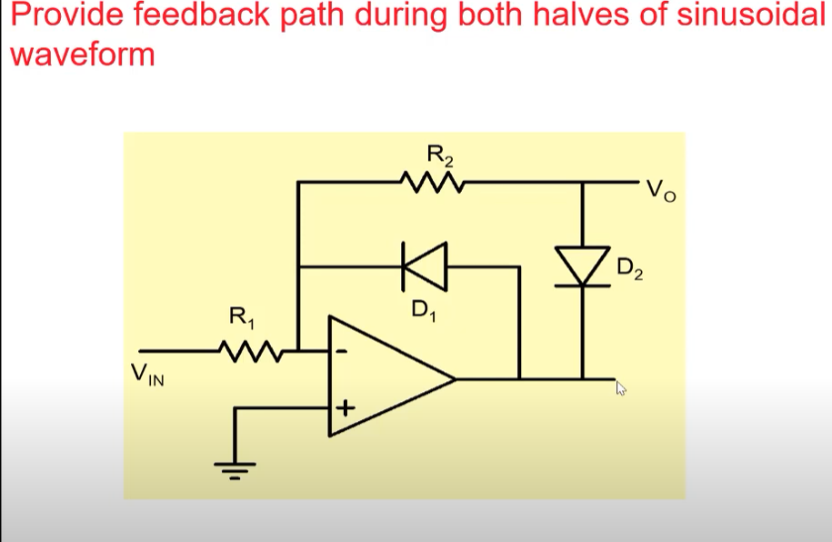
A more optimised circuit nit entirely depending on the diode voltages are using opamps with feedbacks(to prevent large voltage exchange in opamps and to reduce slew rates).
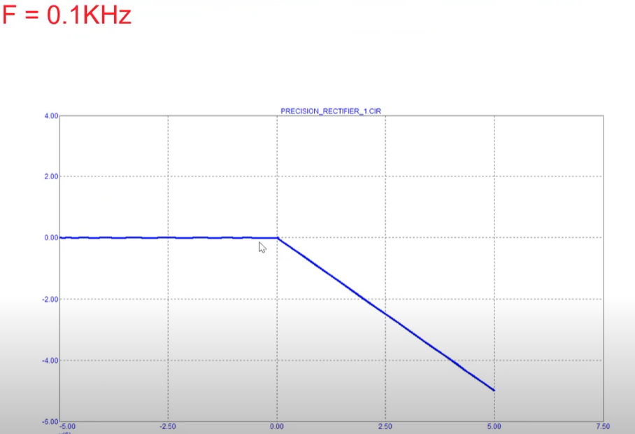
The following characteristics can be obtained using the above circuit.
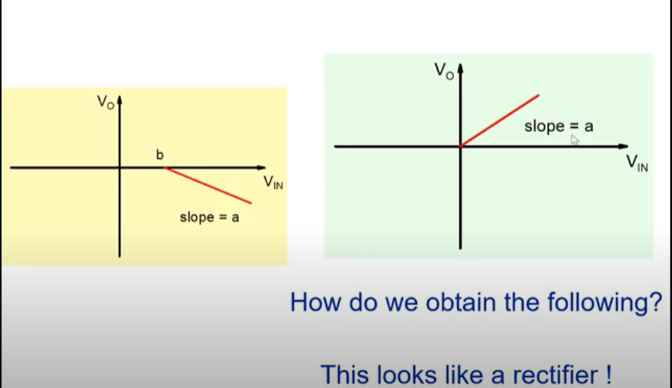
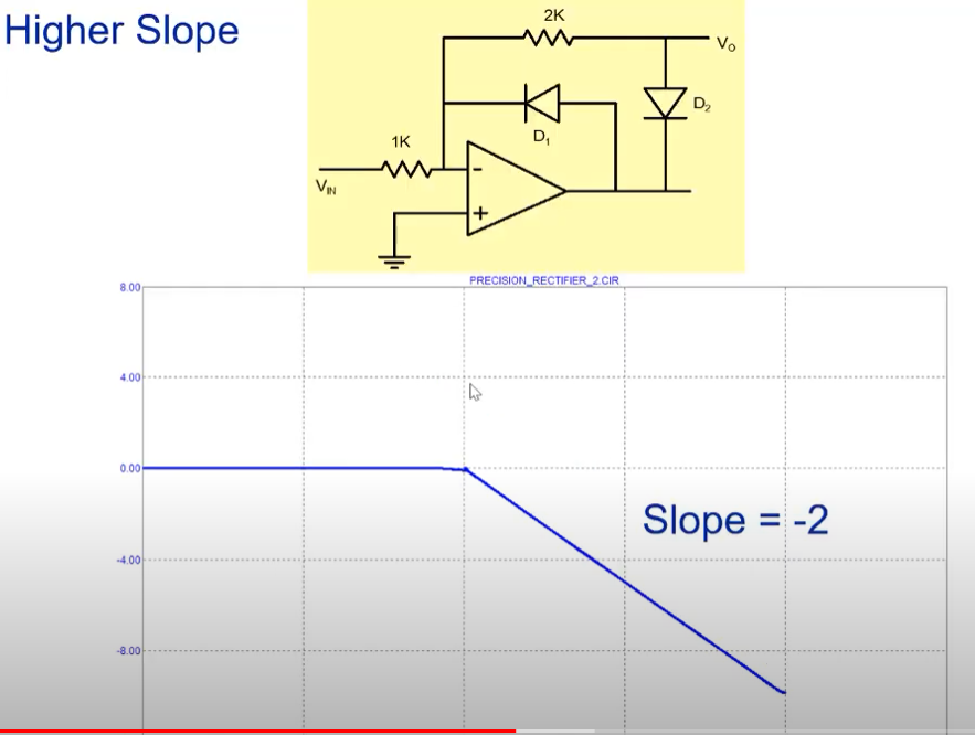
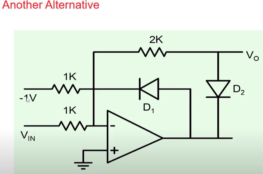
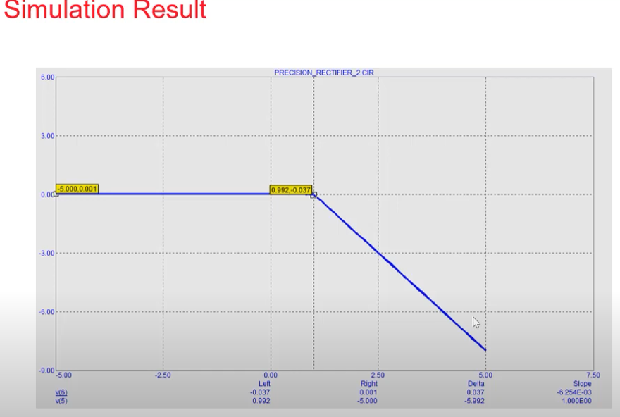
One can also change the slope by tweaking the parameters as shown below.
Shifting the characteristics to the right is obtained using the following circuit
Now in order to design all the three slopes one can make use of the circuit of the following kind:
In order to convert triangular wave to sinusoidal output, we need to take care of the threshold value and gains involved. This can be done using macrosimulation like one shown below
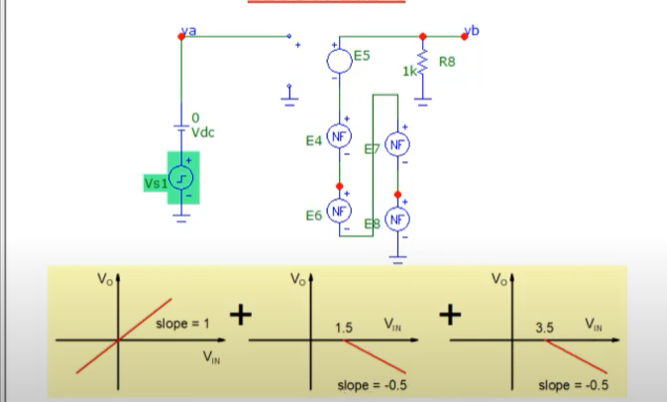
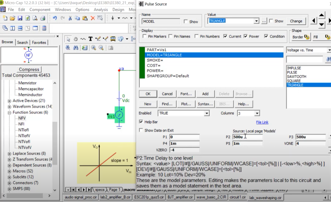
where, Vs1 is the pulse source having triangular form with the following parameters. The on period is $500u$, and the total period is $1m$(frequency of $1Khz$)
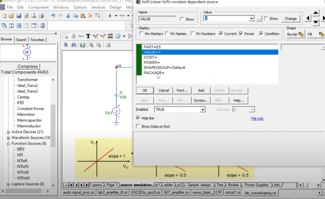
Here, $E5$, is the Voltage controlled voltage source taking control of the slope of $1V$.
The other parts like $E4$ are like functional sources, which takes care of other slope parts. It is like the following:
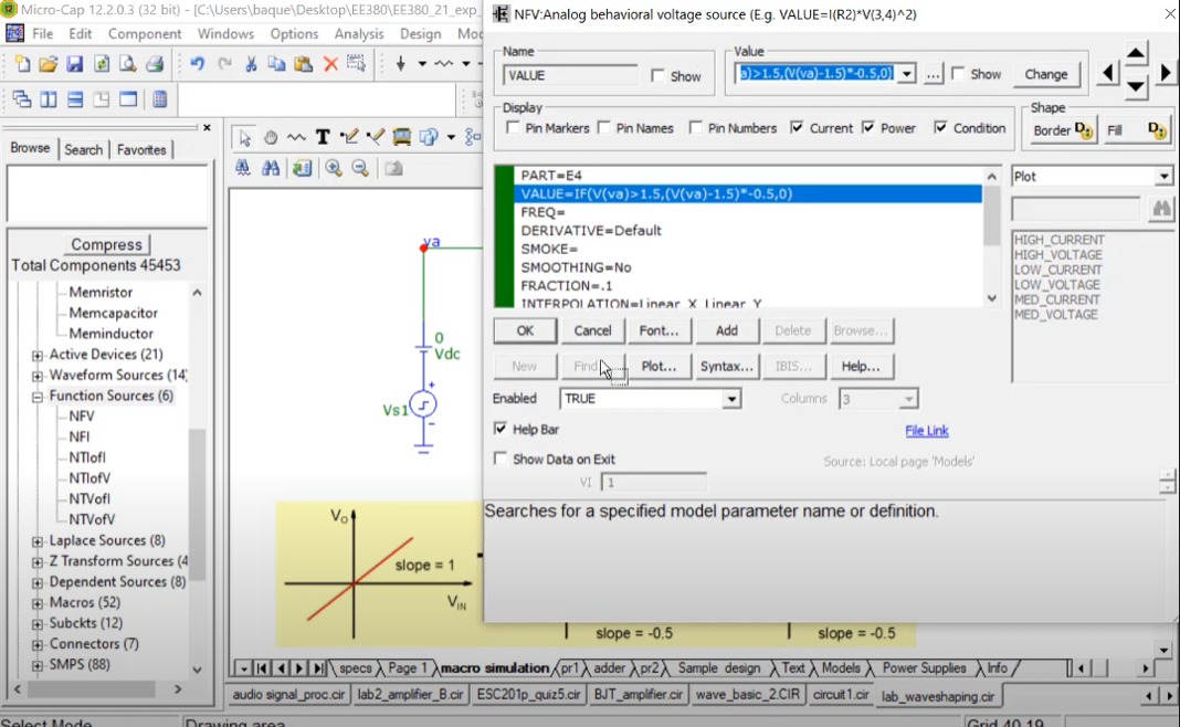
Similarily the value of $E6$ is $IF(V(va)>3.5,(V(va)-3.5)-0.5,0)$, $E7$ is $IF(V(va)<-1.5,(V(va)+1.5)-0.5,0)$, $E8$ is $IF(V(va)<-3.5,(V(va)+3.5)*-0.5,0)$.
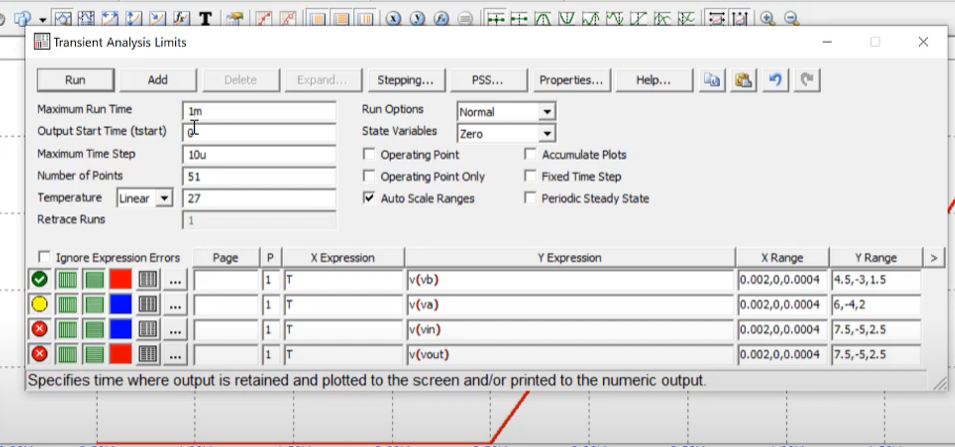
Now, we can do a transient simulation of V(b) and V(a).
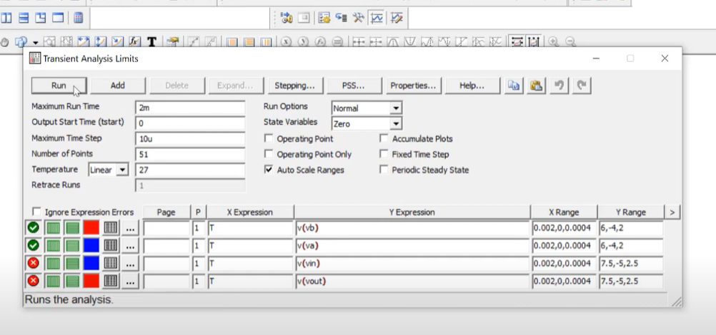
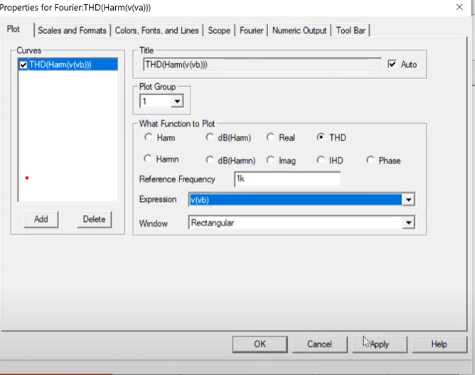
We can also look into the total harmonic distortion by using a fourier window in transient tab.
On chaning simulation time to 1 period, we get the following data
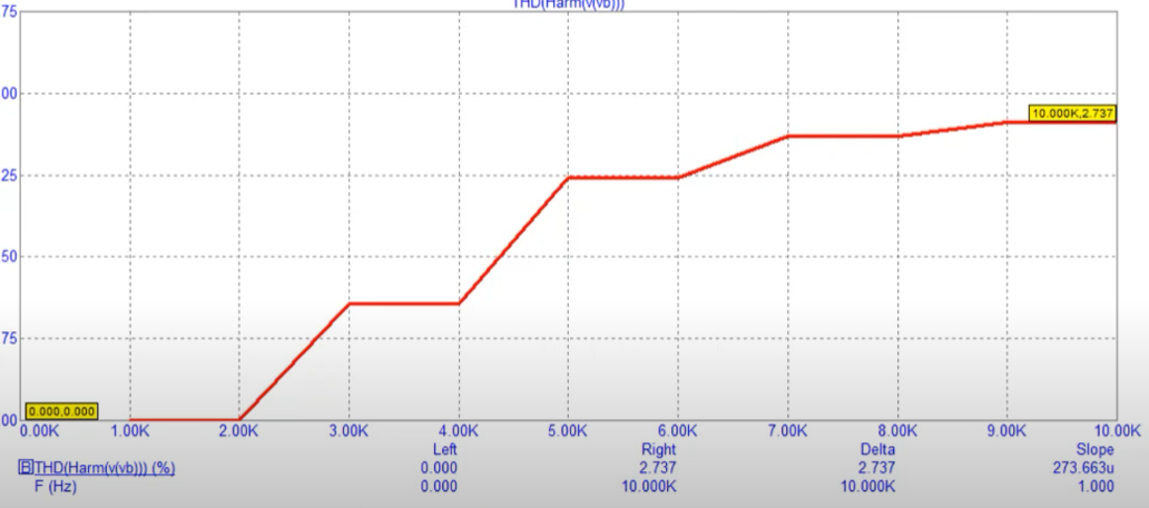
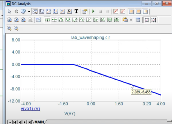
Lower, the final threshold of output gives us a better sinusoid.
To generate a shifted slope we can use the following circuit with the following Vs.
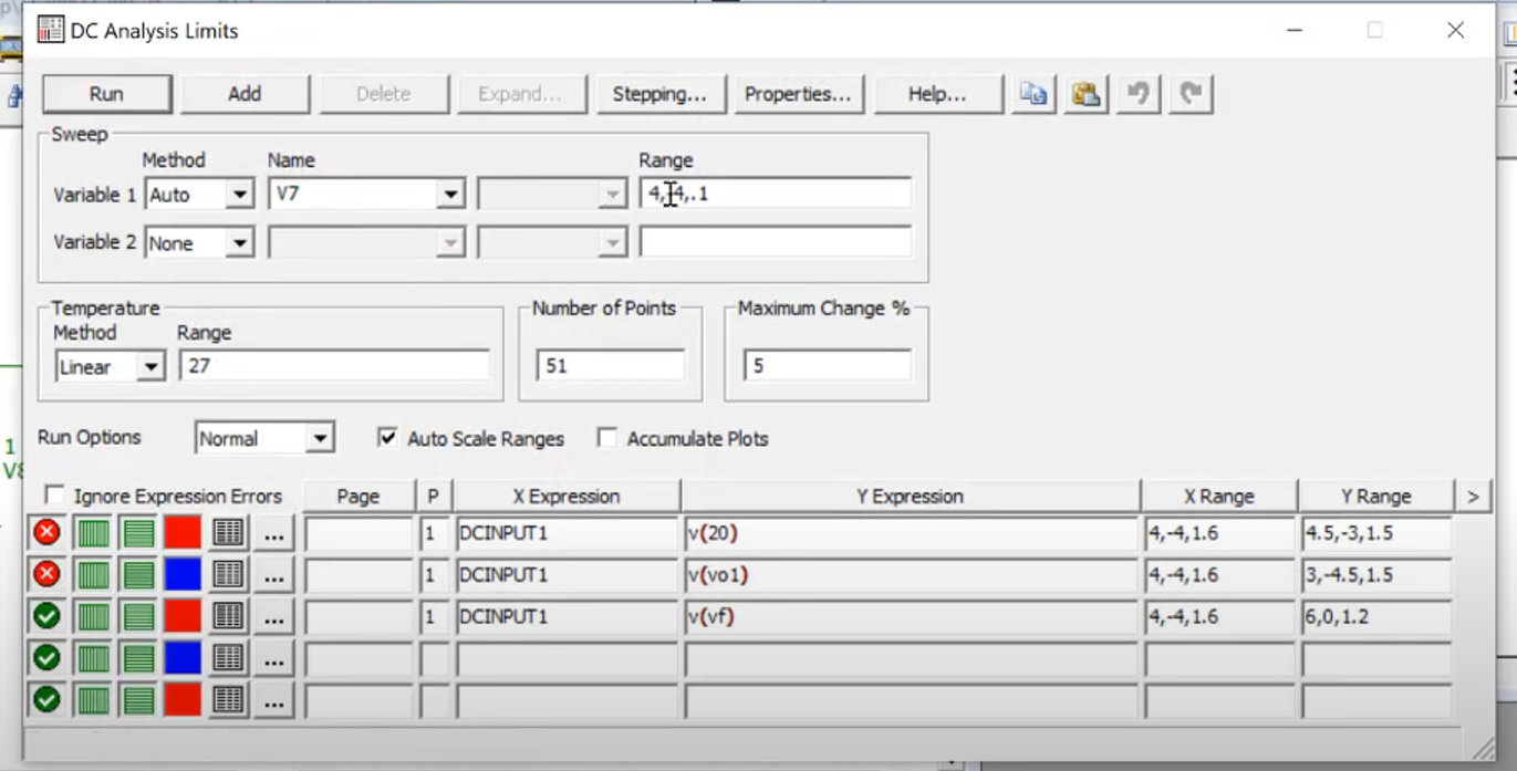
On doing DC analysis, we indeed get the slopes as
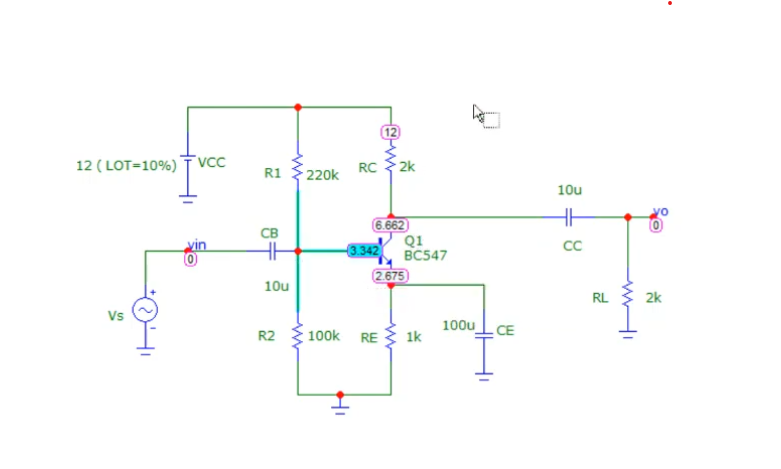
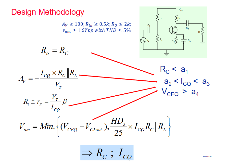
Design a comman emitter amplifier (link)
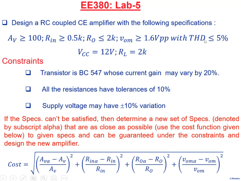
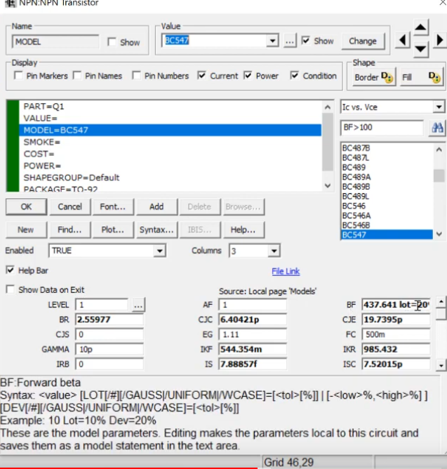
Making the circuit in microcap. Use transistor BC 54
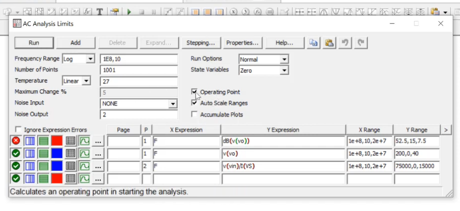
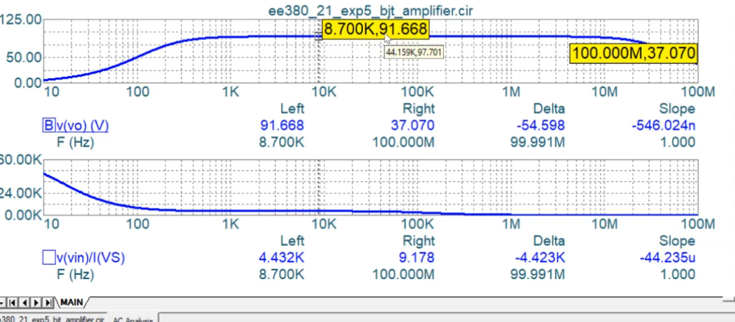
We need to run AC analysis to find small signal gains and Rin and to check whether it matched the desired specifications or not.
The second figure gives Rin while the midband section of the first figure gives gain.
Now, we try to find vo. We use the following Vs for this
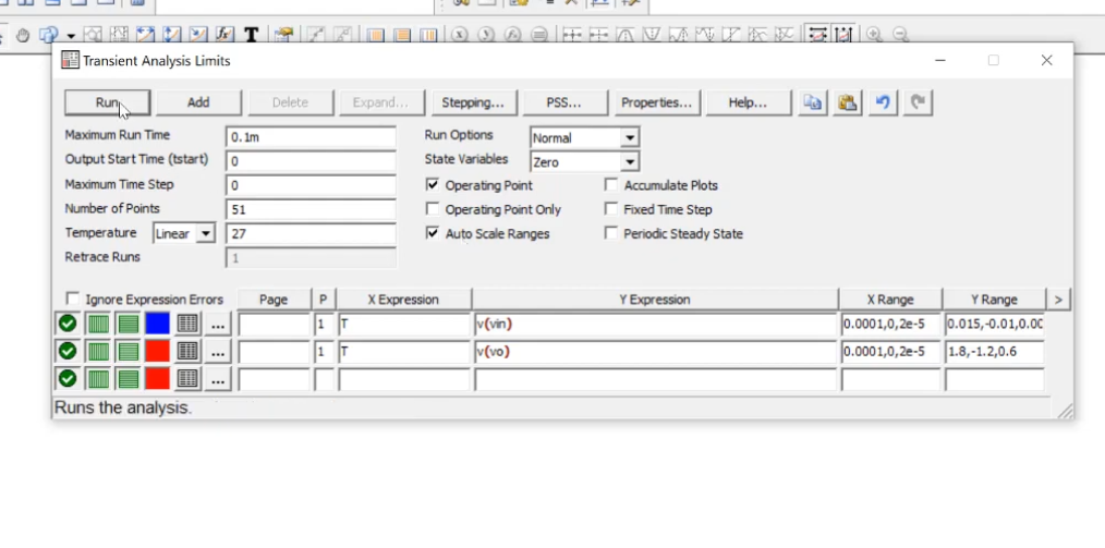
Then we do the transient AC simulation of this setting the max run time as 1/f
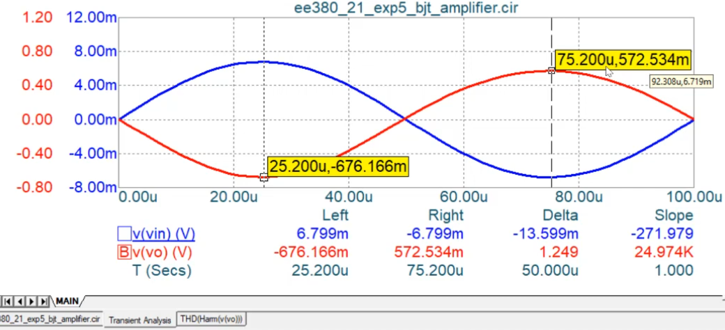
We get the following input output curves. The input is a perfect sinusoid but there is some distortion in the output curve which seems to be an almost sinusoid. We get peak to peak delta as 1.29 but we wanted it to be 1.6
To analyse the distortion, we set up a fourier window as shown
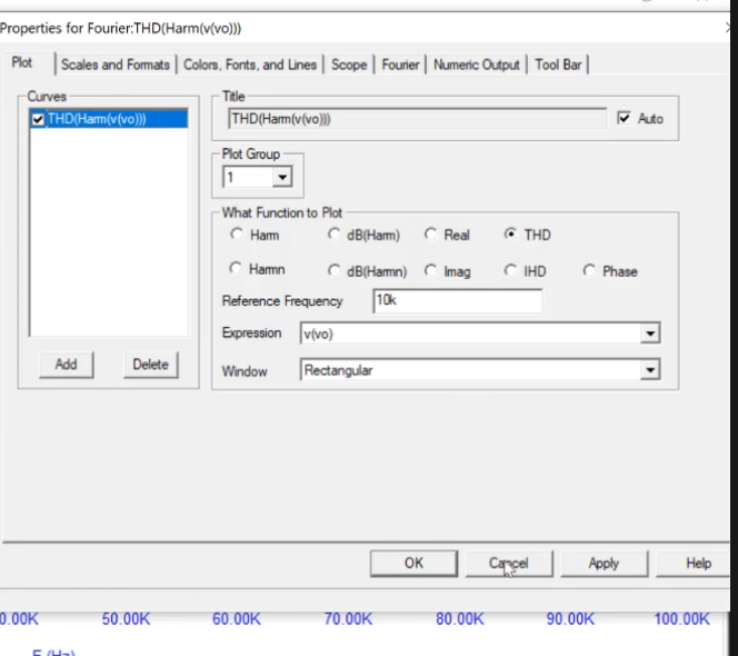
This gives a 5% distortion as shown below. Decreasing the amplitude of input voltage we can reduce the output voltage and also the distortion value. Harmonic distortion primarily depends on input voltage magnitude.
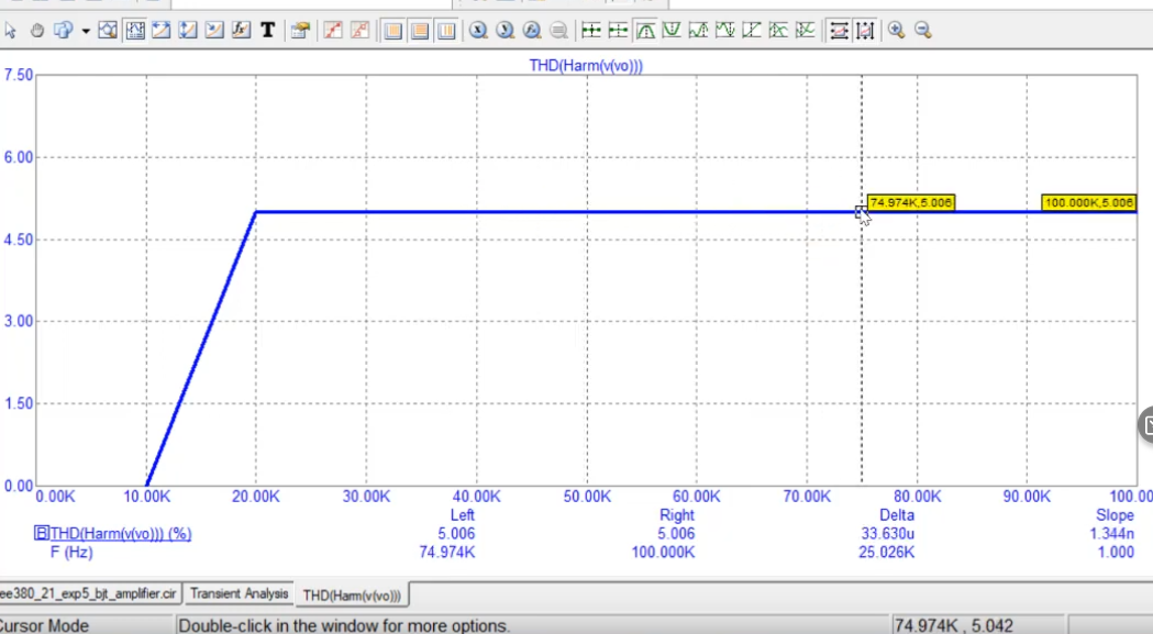
Output resistance is equal to Rc in the above figures.
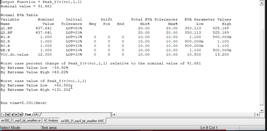
Building an initial design
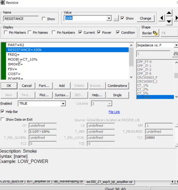
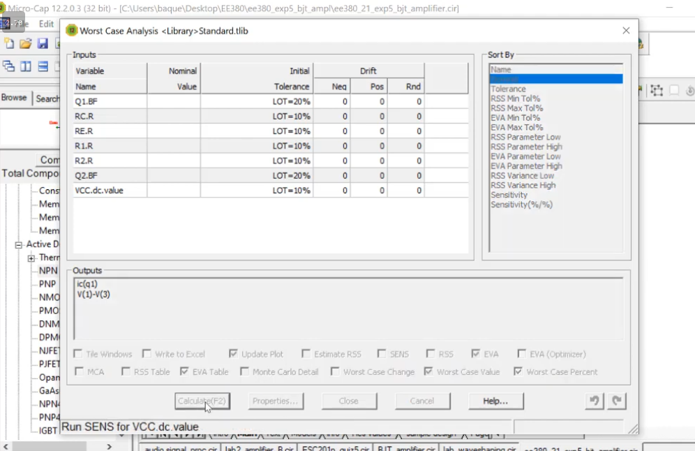
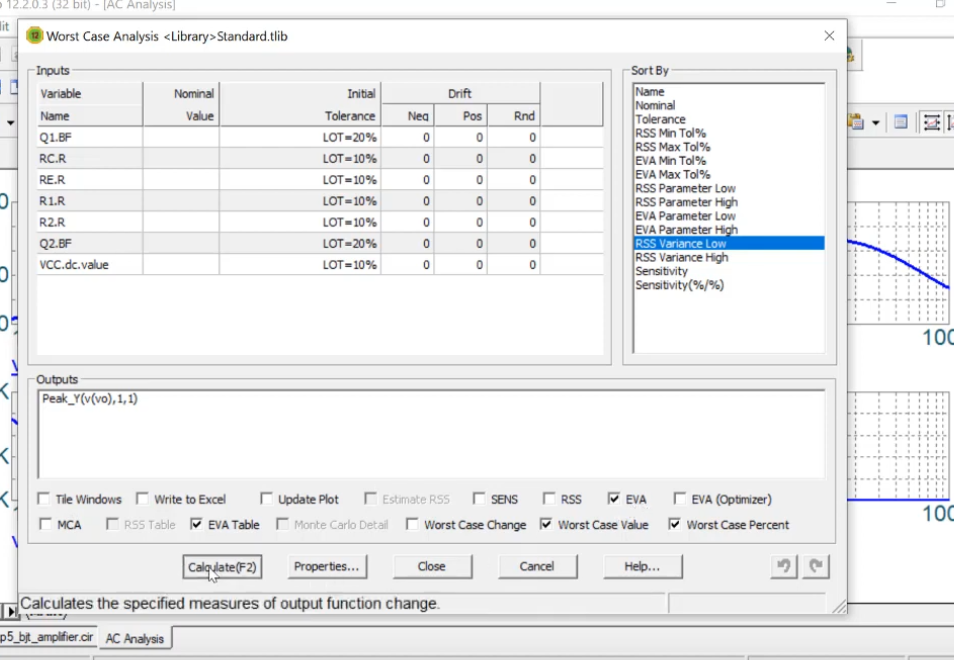
Now we want to take into account the tolerance values.
Choose the following model for resistors. We dont add variation in RL
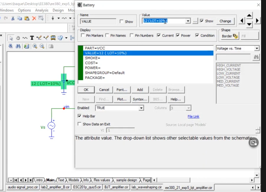
We also add variation in our supply voltage and transistor(for beta)
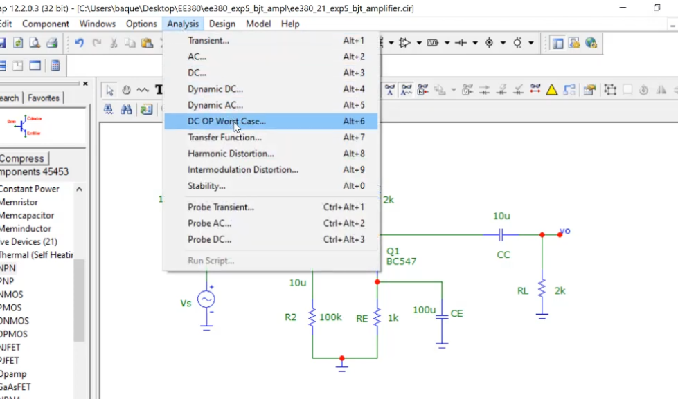
Run worst case analysis to get the extreme values ..
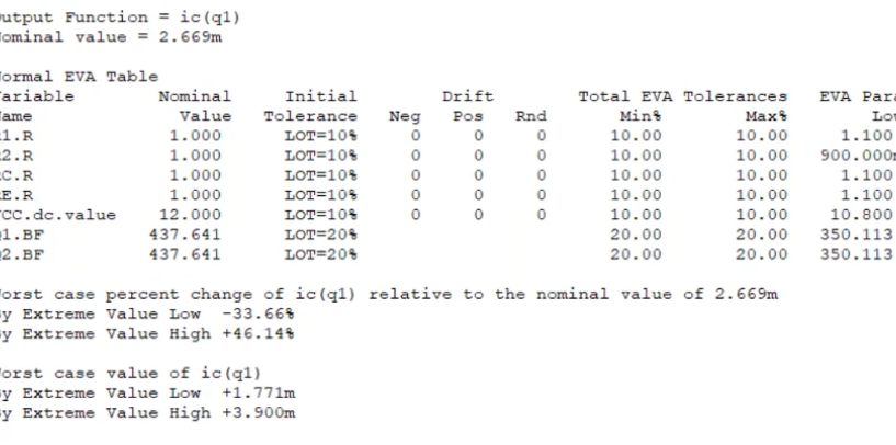
Final result was as
We can also do worst case AC analysis and get the following
We get the following report